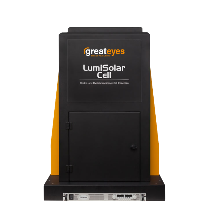
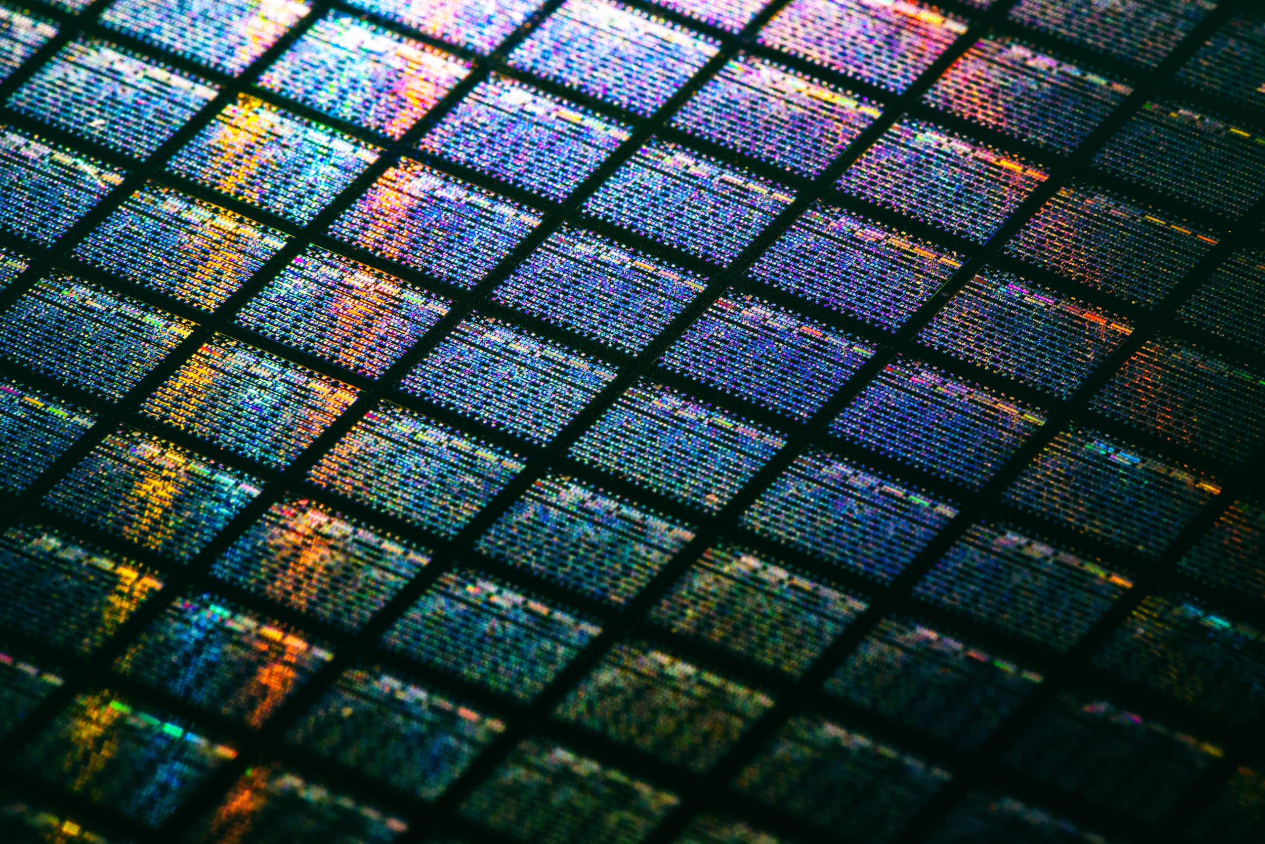
The characterisation methods of the LumiSolarCell EL include various electroluminescence (EL) techniques. These methods encompass EL and reverse-biased EL imaging, which are employed to assess the performance and integrity of solar cells.
Additionally, the measurement of local cell voltage and the mapping of local current density provide detailed insights into the electrical characteristics and efficiency of the cells. An optional technique includes the evaluation of series resistance, further contributing to the comprehensive analysis of the solar cell’s performance.
Outstanding sensitivity and image quality Enabling measurement of multiple PV technologies
Contactless characterisation Non-destructive EL measurement
Award winning system Industry proven all over the globe
Scalable set-up In terms of intensity and supported cell sizes
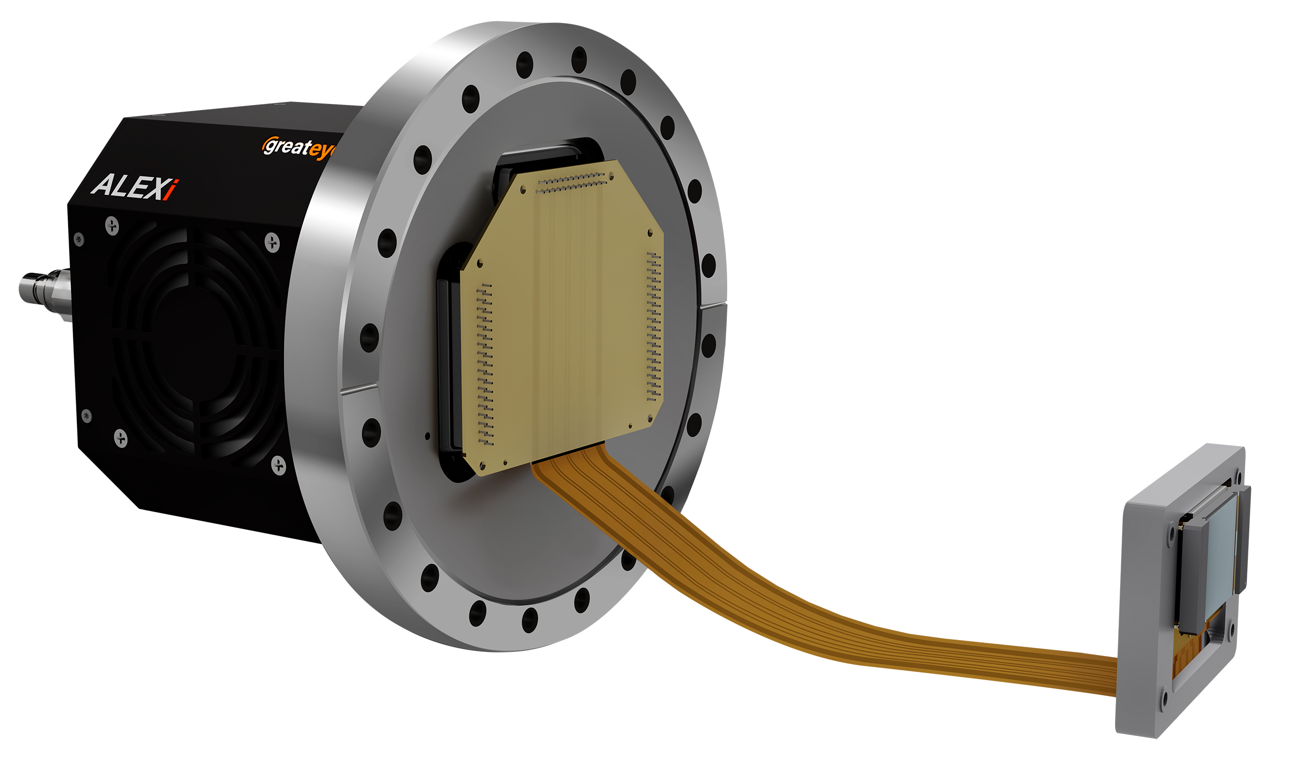
Turnkey system Featuring highly-sensitive scientific CCD-camera
Applications
Inspection of wafers, processed solar cells, and thin film substrates
Research and Development
Characterisation and Qualification
Failure analysis
Identification/sorting of wafers and cells
Specifications
Functionalities
EL, reverse-biased EL
Image size
1024 x 1024 pixel 16-bit, or 2048 x 2048 pixel 16-bit
Image resolution
150 µm/pixel, or 80 µm/pixel
Substrate size
max. 200 mm x 200 mm
Typical exposure times
0.1 sec - 10 sec depending on the substrate and type of measurement
Power supply input
100-240V, 50/60 Hz
EL excitation source
0-80V, 0.9.5A
EL contacting adapter
Adapter for 5 and 6 inch cells (156 mm x 156 mm) included
Flexible design for 2 - 5 bus bars
Vacuum contact adapters for IBC cells available as an option