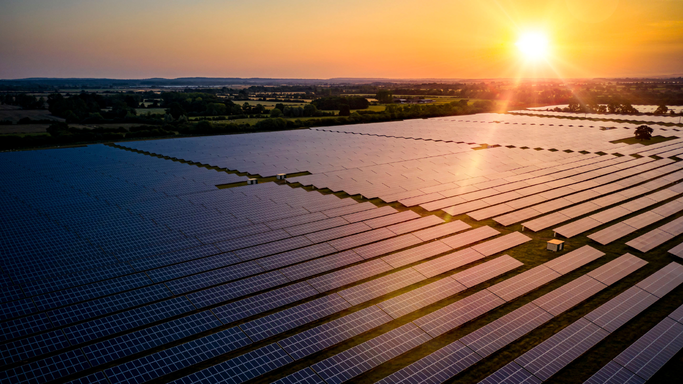
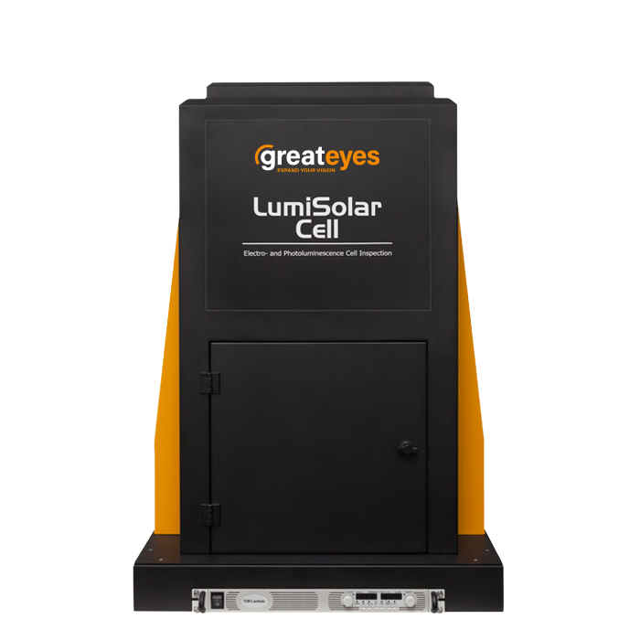
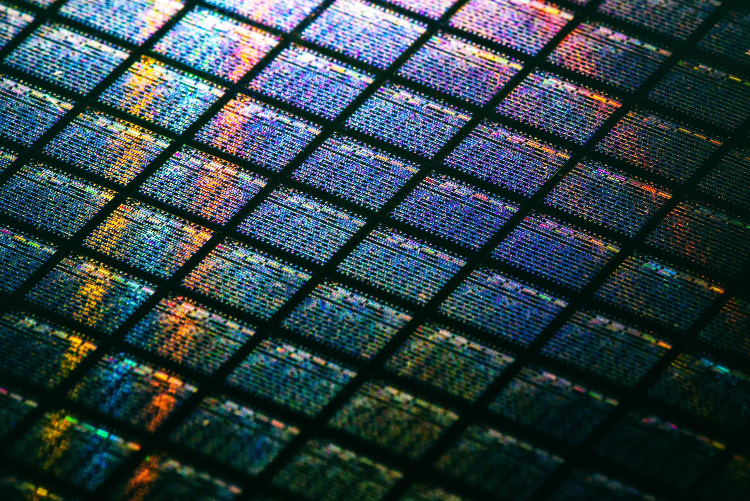
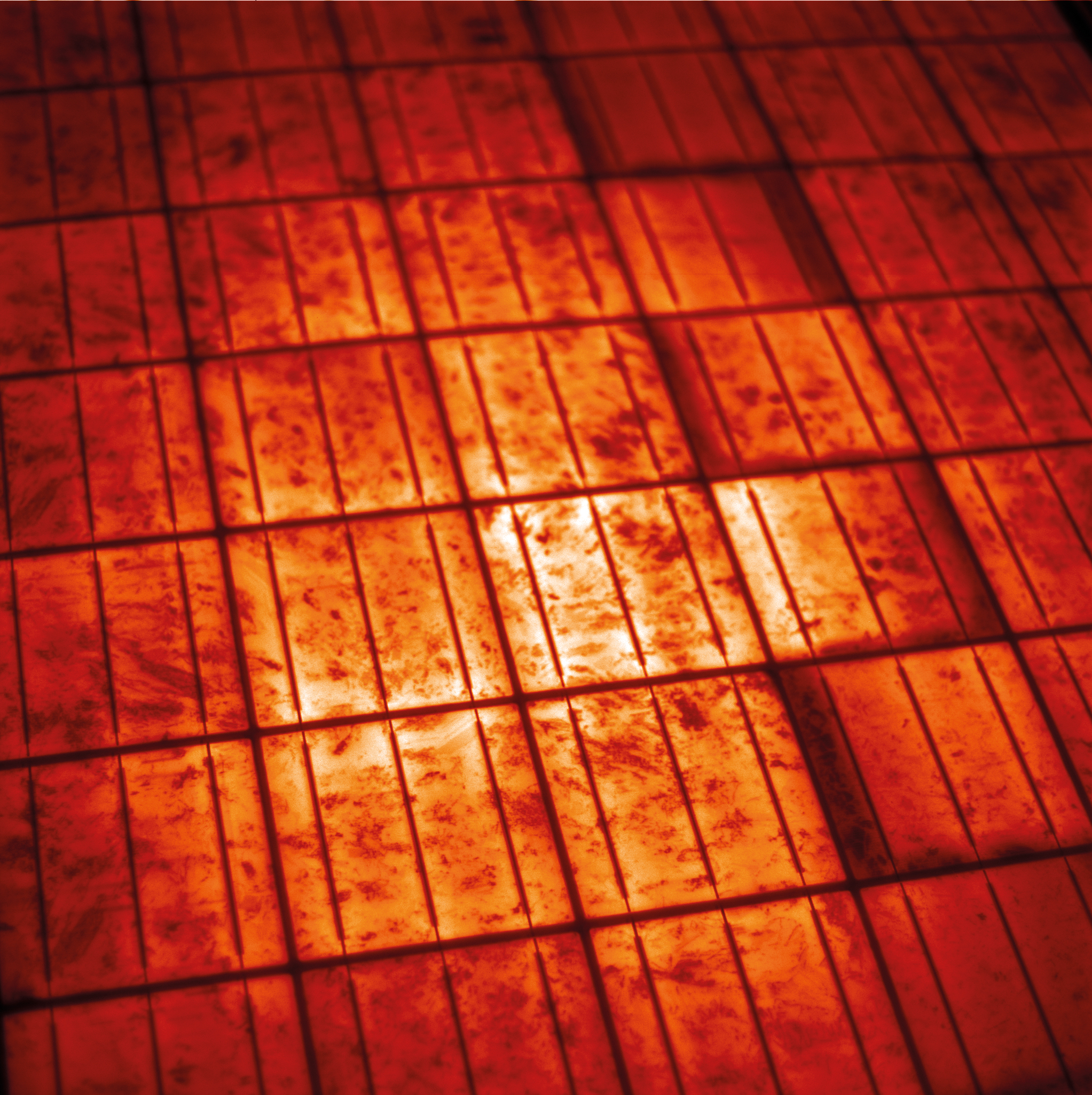
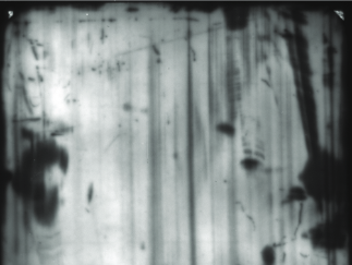
Solar cells and solar modules suffer from a variety of invisible defects which reduce their output power and long-term stability. The highly sensitive Inspection Systems from greateyes can image these problems. This allows you to optimize the production, increase output power, and reduce overall costs.
Get in touch with our experts to find the most qualified greateyes system for your application.
Standard Thermal Cycling Test S. Roy, S. Kumar, R. Gupta. Investigation and analysis of finger breakages in commercial crystalline silicon photovoltaic modules under standard thermal cycling test. Engineering Failure Analysis, 2019, Volume 101, Pages 309-319
PV Field Applications U. Jahn et al. Review on IR and EL Imaging for PV Field Applications.International Energy Agency, Photovoltaic Power Systems Programme, Report IEA-PVPS T13-10:2018, March 2018
Crystalline Silicon As-Cut Wafers M. Regehly, R. Kemmler. LED-Based Photoluminescence Inspection of Crystalline Silicone As-Cut Wafers. Poster at the EU PVSEC 2015, Hamburg
Degradation C. Peike, S. Hoffmann, M. Heck, T. Kaltenbach, K.-A. Weiß, M. Köhl. Nondestructive Determination of Climate-Specific Degradation Patterns for Photovoltaic-Module Encapsulation. Energy Technology, 2014, Volume 2, Issue 1, pages 121–129C. Peike, S. Hoffmann, P. Hülsmann, B. Thaidigsmann, K.A. Weiβ, M. Koehl, P. Bentz. Origin of damp-heat induced cell degradation. Solar Energy Materials and Solar Cells, 2013, Volume 116, Pages 49–54
Defect Detection A. Mansouri, M. Zettl, O. Mayer, M. Lynass, M. Bucher, O. Stern, C. Heller, E. Mueggenburg. Defect detection in photovoltaic modules using electroluminescence imaging. 27th EU PVSEC, 2012M. Regehly, J. Penlington. Im Einsatz für mehr Strom. Elektrolumineszenz-Inspektion von Solarzellen und -modulen, Inspect-Online, 3/2012