SYSTEM SERIES: LumiSolar Cell
SYSTEM SERIES: LumiSolar Cell
System Families
SYSTEM SERIES: LumiSolar Cell
SYSTEM SERIES: LumiSolar Cell
Camera Portfolio
Camera Families
Camera Series
LEED Imaging
Low Energy Electron Diffraction technique
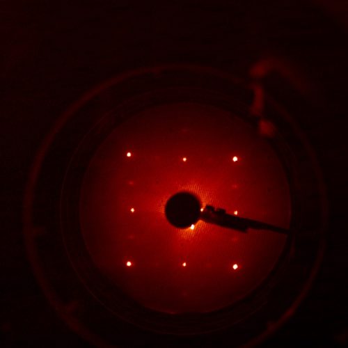
LEED (Low Energy Electron Diffraction) imaging is a technique used to determine the atom formation on surface structures and thin films of crystalline materials. For this purpose, a bombardment with a collimated beam of low energy electrons on the probe material is arranged. The electrons are scattered on the surface and are observable as spots on a fluorescent screen. The example below shows a sample material that was bombarded with electrons. The resulting diffraction pattern has been recoded by the camera GE 1024 1024 BI MID. The high sensitivity of this camera allows to detect weak diffraction spots.

Recommended Products
References
greateyes GmbH
Ludwig-Boltzmann-Straße 3
12489 Berlin
Germany

Ludwig-Boltzmann-Straße 3
12489 Berlin